Difference between revisions of "MainPage:Nuclear:NPS:PWO:CrystalLOG:SICCAJ32"
Jump to navigation
Jump to search
| Line 18: | Line 18: | ||
! "background:#f5f5f5;" style="text-align:center; background:lavender; font-weight:bold; width:75%;" | Comments | ! "background:#f5f5f5;" style="text-align:center; background:lavender; font-weight:bold; width:75%;" | Comments | ||
|- | |- | ||
| − | | 03/17/2016 || Pictures || Documentation of crystal's conditions as it arrived at CUA. | + | | 03/17/2016 || Salina || Pictures || Documentation of crystal's conditions as it arrived at CUA. |
|- | |- | ||
| − | | 03/18/2016 || Thermal annealing || Ramp up at 18oC/hour up to 200oC. Stays for 10 hours and ramp down at 18oC/hour. | + | | 03/18/2016 || Salina || Thermal annealing || Ramp up at 18oC/hour up to 200oC. Stays for 10 hours and ramp down at 18oC/hour. |
|- | |- | ||
| − | | 04/15/2016 || Light Yield || Run 3191: crystal wrapped with ~5 layers of teflon tape and 2 layers of black tape. Steps of 20min, 1cm. T=18oC. LY = 18.41 pe/MeV. | + | | 04/15/2016 || Salina || Light Yield || Run 3191: crystal wrapped with ~5 layers of teflon tape and 2 layers of black tape. Steps of 20min, 1cm. T=18oC. LY = 18.41 pe/MeV. |
|- | |- | ||
| − | | 05/17/2016 || Transverse Transmittance || At the center of the crystal, every nm from 200nm until 800nm. Sample: 1348 | + | | 05/17/2016 || Salina || Transverse Transmittance || At the center of the crystal, every nm from 200nm until 800nm. Sample: 1348 |
|- | |- | ||
| − | | 05/20/2016 || Transverse Transmittance Scan || Wavelengths: 360nm, 420nm, 620nm. Sampling period: 0.6s, moving motor at 2mm/s. | + | | 05/20/2016 || Salina ||Transverse Transmittance Scan || Wavelengths: 360nm, 420nm, 620nm. Sampling period: 0.6s, moving motor at 2mm/s. |
|- | |- | ||
| − | | 07/07/2016 || Longitudinal Transmittance Scan || Wavelengths: 200-800 nm. Sampling period: 0.6s, moving motor at 2mm/s. | + | | 07/07/2016 || Summer Students ||Longitudinal Transmittance Scan || Wavelengths: 200-800 nm. Sampling period: 0.6s, moving motor at 2mm/s. |
|- | |- | ||
| − | | 07/27/2016 || Light Yield || Run 3274. 300ns gw. >50,000 incidents ~3 layers of teflon tape ~1 layer of electrical. | + | | 07/27/2016 || Summer Students || Light Yield || Run 3274. 300ns gw. >50,000 incidents ~3 layers of teflon tape ~1 layer of electrical. |
| − | + | |- | |
| + | |01/06/2017 || Rich/TH || Light Yield || 3 layers teflon, 2 layers black tape, run 3534, result: 8.07 pe/MeV. | ||
| + | |- | ||
| + | |01/06/2017 || Rich/TH || Transverse Transmittance || before irradiation. | ||
| + | |- | ||
| + | |01/06/2017 || Rich/TH || Transverse Transmittance || before irradiation. | ||
| + | |- | ||
| + | |01/06/2017 || Rich/TH || Transverse+Longitudinal Transmittance || after irradiation. | ||
| + | |- | ||
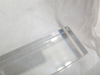
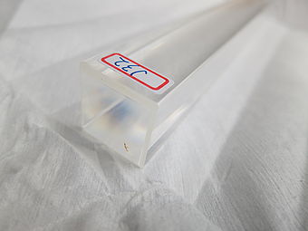
| + | |01/06/2017 || Rich/TH || Crystal accident - two pieces chip off at one end (see pictures below). | ||
|} | |} | ||
Revision as of 00:50, 8 January 2017
| ⇐ Back to Crystal LOG |
| ⇐ Back to Neutral Particle Spectrometer |
| ⇐ Back to the Main_Page |
Time LOG
| Date | Description | Comments | |
|---|---|---|---|
| 03/17/2016 | Salina | Pictures | Documentation of crystal's conditions as it arrived at CUA. |
| 03/18/2016 | Salina | Thermal annealing | Ramp up at 18oC/hour up to 200oC. Stays for 10 hours and ramp down at 18oC/hour. |
| 04/15/2016 | Salina | Light Yield | Run 3191: crystal wrapped with ~5 layers of teflon tape and 2 layers of black tape. Steps of 20min, 1cm. T=18oC. LY = 18.41 pe/MeV. |
| 05/17/2016 | Salina | Transverse Transmittance | At the center of the crystal, every nm from 200nm until 800nm. Sample: 1348 |
| 05/20/2016 | Salina | Transverse Transmittance Scan | Wavelengths: 360nm, 420nm, 620nm. Sampling period: 0.6s, moving motor at 2mm/s. |
| 07/07/2016 | Summer Students | Longitudinal Transmittance Scan | Wavelengths: 200-800 nm. Sampling period: 0.6s, moving motor at 2mm/s. |
| 07/27/2016 | Summer Students | Light Yield | Run 3274. 300ns gw. >50,000 incidents ~3 layers of teflon tape ~1 layer of electrical. |
| 01/06/2017 | Rich/TH | Light Yield | 3 layers teflon, 2 layers black tape, run 3534, result: 8.07 pe/MeV. |
| 01/06/2017 | Rich/TH | Transverse Transmittance | before irradiation. |
| 01/06/2017 | Rich/TH | Transverse Transmittance | before irradiation. |
| 01/06/2017 | Rich/TH | Transverse+Longitudinal Transmittance | after irradiation. |
| 01/06/2017 | Rich/TH | Crystal accident - two pieces chip off at one end (see pictures below). |

